2026
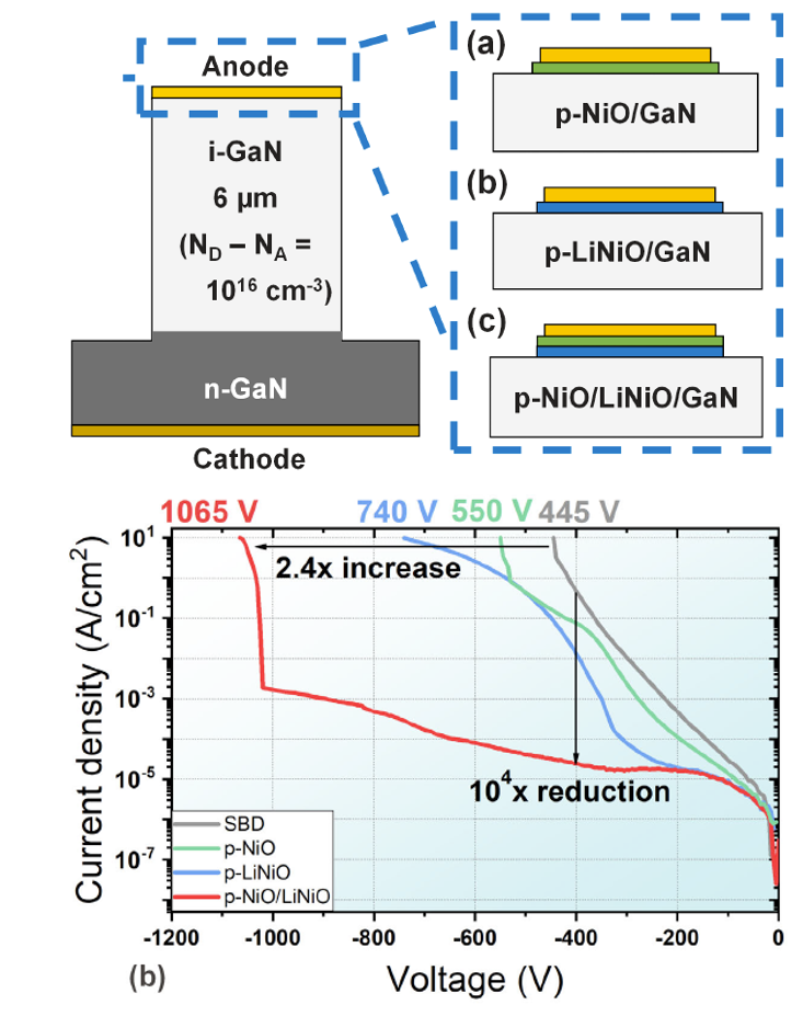
Z. Hao, A. Floriduz, Y. Zong and E. Matioli, “Polarization Enhanced GaN SBDs With p-NiO/LiNiO Junction Termination Extensions Achieving 1 kV Breakdown Voltage,” IEEE Electron Device Letters, vol. 47, no. 4, pp. 704–707, 2026.
2025
Z. Hao, A. Floriduz, Y. Zong, U. Choi, M. Mensi and E. Matioli, “p-NiO/LiNiO-GaN Heterojunctions: A Potential Alternative to p-GaN for Advanced Devices,” IEEE Electron Device Letters, vol. 46, no. 5, pp. 729–732, 2025.
2024
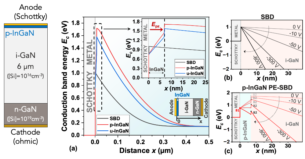
A. Floriduz, Z. Hao and E. Matioli, “Polarization-Enhanced GaN Schottky Barrier Diodes: Ultra-Thin InGaN for High Breakdown Voltage and Low Ron,” IEEE Electron Device Letters, vol. 45, no. 7, pp. 1121–1124, 2024.
2024
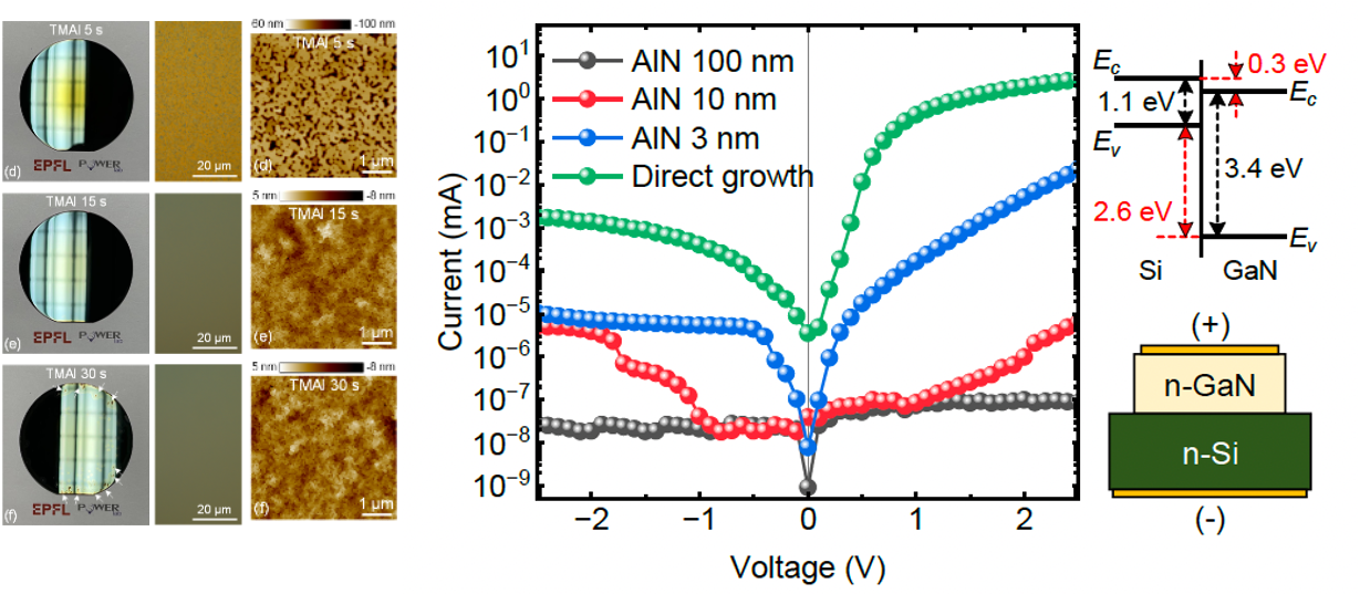
A. Floriduz, U. Choi, and E. Matioli, “Direct high-temperature growth of GaN on Si using trimethylaluminum preflow enabling vertically-conducting heterostructures,” Jpn. J. Appl. Phys., vol. 63, no. 6, p. 060904, 2024.
2022
A. Floriduz and E. Matioli, “GaN growth on ScAlMgO₄ substrates via thermally-dewetted thin Al films,” Jpn. J. Appl. Phys., vol. 61, p. 118003, 2022.
2021
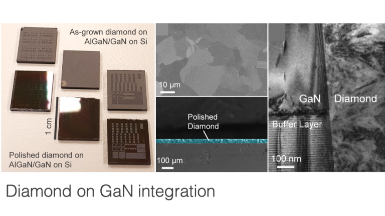
R. Soleimanzadeh, M. Naamoun, A. Floriduz, R. A. Khadar, R. van Erp and E. Matioli, “Seed Dibbling Method for the Growth of High-Quality Diamond on GaN,” ACS Applied Materials & Interfaces, vol. 13, no. 36, pp. 43516–43523, 2021.
2021
R. A. Khadar, A. Floriduz, T. Wang and E. Matioli, “p-NiO junction termination extensions for GaN power devices,” Appl. Phys. Express, vol. 14, 071006, 2021.
2020
R. Soleimanzadeh, M. Naamoun, R. A. Khadar, R. van Erp and E. Matioli, “H-Terminated Polycrystalline Diamond p-Channel Transistors on GaN-on-Silicon,” IEEE Electron Device Letters, vol. 41, no. 1, pp. 119–122, 2020.
2019
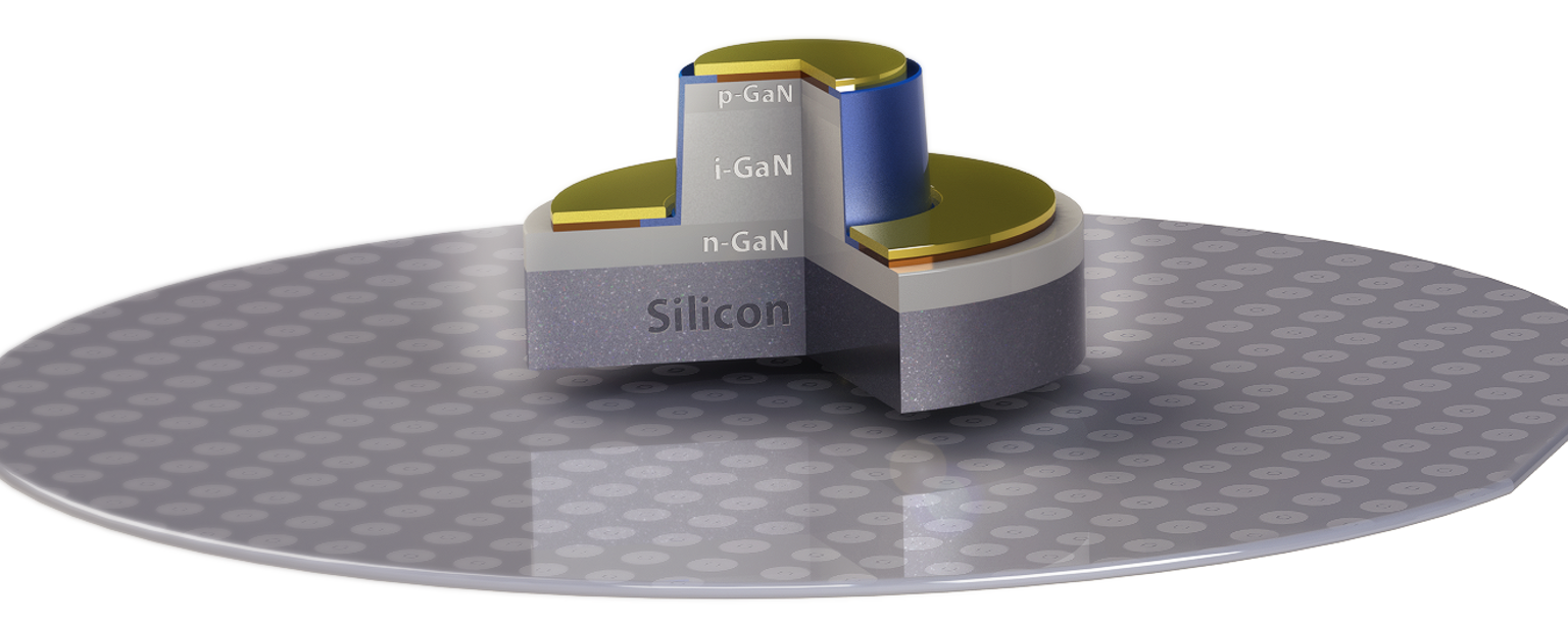
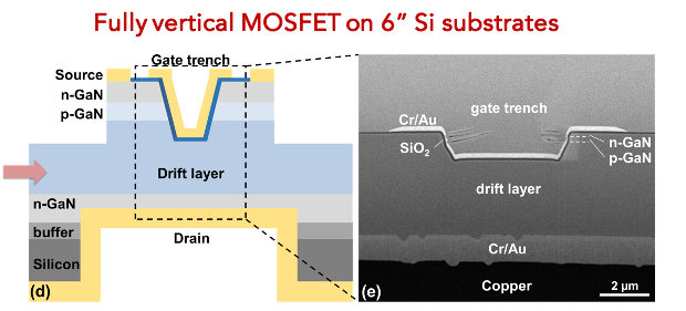
R. A. Khadar, …, E. Matioli, “Fully-vertical GaN-on-Si power MOSFETs,” IEEE Electron Device Letters, 2019.
2018
R. A. Khadar, …, E. Matioli, “820 V GaN-on-Si Quasi-Vertical P-i-N Diodes with BFOM of 2.0 GW/cm²,” IEEE Electron Device Letters, 2018. (IEEE EDL Editor’s Pick)
2018
C. Liu, …, E. Matioli, “GaN-on-Si Quasi-Vertical Power MOSFETs,” IEEE Electron Device Letters, 2018.