POWERlab / Research / Ultrafast Electronics

Ultrafast electronics & THz devices

Novel device concepts — from nanoplasma switches to electronic metadevices — that break classical speed limits, enabling picosecond switching, terahertz-range cutoff frequencies, and new frontiers in 6G communications. Published in Nature and Nature Electronics.

The challenge

Beyond classical device limits

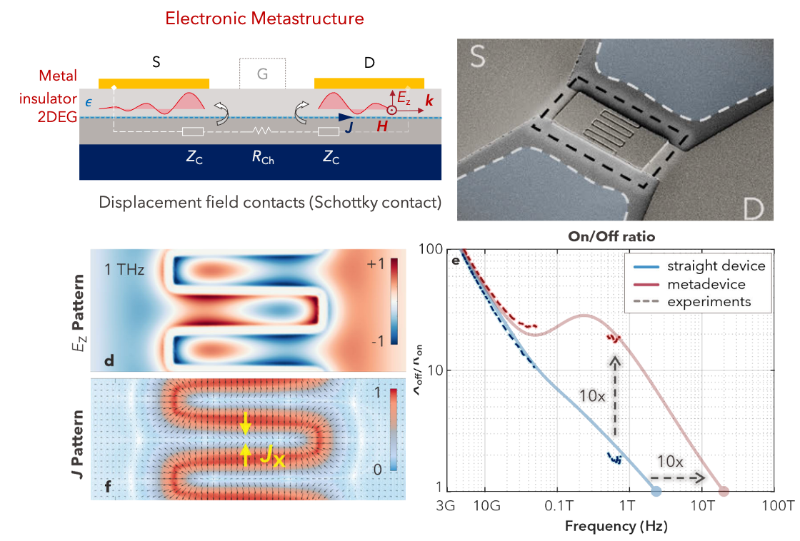
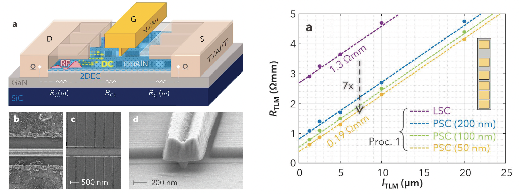
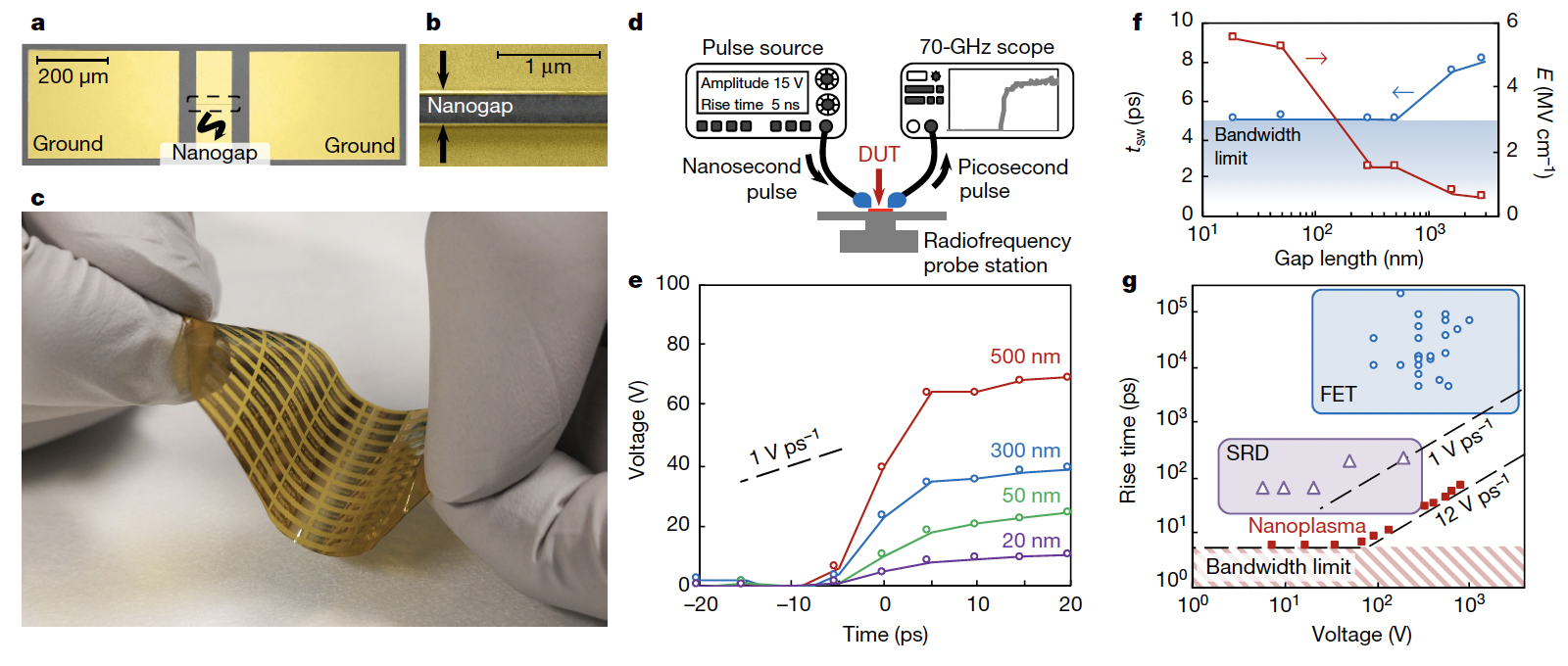
The evolution of electronics has generally relied on reducing device size to increase speed and integration. However, as the channel length shrinks, classic electronic devices face fundamental limitations that hinder exploiting materials to their ultimate potential. The benefits of scaling are counterbalanced by parasitic resistances and capacitances, which limit frequency and output power.

In our group, we challenge such traditional limitations by investigating novel types of devices, based on new physical principles and materials, that could enable the next generation of ultrafast semiconductor devices.

Ultrafast electronics concept
Novel device concepts

Key innovations

3 device concepts
Core concept

Electronic metadevices for terahertz applications

In the electronic metadevice concept, we proposed the microscopic manipulation of radiofrequency fields, like in metamaterials in optics but applied to electronics, in which a metamaterial resonates with the 2DEG to form an active metadevice. The devices operate on the basis of electrostatic control of collective electromagnetic interactions at deep subwavelength scales, as an alternative to controlling the flow of electrons in traditional devices. This resulted in a huge current confinement in the active region of the device, significantly reducing the effective contact resistance and increasing their cutoff frequency by over an order of magnitude. Metadevices are controllable — they can be rapidly turned on and off with a DC bias, which is conceptually different from optical metamaterials, which offer no control. This enables a new class of electronic devices with cut-off frequency figure-of-merit well beyond 10 THz, record high conductance values, extremely high breakdown voltages, and picosecond switching speeds — setting the stage for the next generation of ultrafast semiconductor devices.

Electronic metadevice structure and THz performance
RF power amplifiers

Regrowth-free GaN RF HEMTs achieving fmax of 403 GHz

A key challenge in sub-THz GaN RF HEMTs is achieving low contact resistance (RC) without costly regrowth processes that require high temperatures and MOCVD or MBE, which complicate fabrication and can damage sensitive RF heterostructures. We demonstrated a periodic side contact (PSC) scheme that transforms conventional linear contacts into a configuration with far better overall RC, yielding values as low as 0.15 Ω·mm — comparable to the best regrown contacts. The technique is based on an Au-free, low-temperature process below 500 °C, producing extremely smooth edges that enable sub-500 nm channel scaling. Using this approach, we demonstrated regrowth-free InAlN/GaN RF HEMTs with fmax of 403 GHz and a peak transconductance of 675 mS/mm — results comparable to the best GaN HEMTs with similar geometry, highlighting the enormous potential of periodic contact structures for high-performance RF and sub-THz devices.

Periodic side contact GaN RF HEMT — schematic and SEM images
Picosecond switching

Nanoplasma-enabled picosecond switches

We proposed an on-chip all-electronic device concept based on integrated nano-scale plasma that enabled picosecond switching of high-power electric signals. The devices produced ultrafast switching speed, higher than 10 V/ps, about two orders of magnitude larger than that of field-effect transistors and more than 10-fold faster than the current fastest electronic switch. By coupling a nanoplasma switch to a judiciously designed THz resonator, we achieved a chip-scale, high-power THz source operating at room temperature, with state-of-the-art peak power of 2 W at 0.4 THz. This represented a Pf² > 300 mW·THz² — significantly larger, by more than 2 orders of magnitude, than the state of the art in solid-state electronics. The ease of integration and compactness of the nanoplasma switches open new horizons in imaging, sensing, communications, and biomedical applications.

Nanoplasma switch concept and THz generation
ERC Advanced Grant 2024

POWERED — Ultrafast electronics vision

Our group has recently been awarded a 2024 ERC Advanced Grant which also encompasses ultrafast electronics. The project, named POWERED, aims to significantly increase output power and linearity in GaN RF devices using fundamentally different methods from conventional down-scaling methods, leading to much higher efficiencies and direct integration into RF circuits.

European Research Council logo
Selected references

Key publications

2025

M. Rezaei, H. Zhu, A. Esteghamat and E. Matioli, “Regrowth-Free GaN RF HEMTs Achieving fmax of 403 GHz via Periodic Contact Structures,” IEEE Electron Device Letters, 2025.

2025

M. Rezaei, A. Esteghamat and E. Matioli, “Terahertz Electronic Metadevices: Principles Behind the Ultra-High Cutoff Frequency,” IEEE Electron Device Letters, vol. 46, no. 11, pp. 1986–1989, 2025.

2024

M. Rezaei and E. Matioli, “Chip-Scale Watt-Range Terahertz Generation Based on Fast Transition in Nanoplasma Switches,” IEEE Electron Device Letters, vol. 45, no. 6, pp. 1072–1075, 2024.

2023

M. S. Nikoo and E. Matioli, “Electronic metadevices for terahertz applications,” Nature 614, 451–455, 2023.

2021

M. S. Nikoo, A. Jafari, R. Van Erp and E. Matioli, “Kilowatt-range Picosecond Switching Based on Microplasma Devices,” IEEE Electron Device Letters, 2021.

2020

M. S. Nikoo, A. Jafari, N. Perera, M. Zhu, G. Santoruvo and E. Matioli, “Nanoplasma-Enabled Picosecond Switches for Ultra-Fast Electronics,” Nature, 2020.

2020

G. Santoruvo, M. Samizadeh Nikoo and E. Matioli, “Broadband Zero-Bias RF Field-Effect Rectifiers Based on AlGaN/GaN Nanowires,” IEEE Microwave and Wireless Components Letters, 2020.

2017

G. Santoruvo and E. Matioli, “In-Plane-Gate GaN Transistors for High-Power RF Applications,” IEEE Electron Device Letters, 2017.

← Back to all research areas