POWERlab / Research / Power Devices

Power electronic devices

Novel multi-channel architectures, slanted tri-gates, and intrinsic polarization superjunctions that set world records for on-resistance, breakdown voltage, and figure of merit — from lateral and vertical GaN HEMTs to ultra-wide-bandgap integration. Backed by a 2024 ERC Advanced Grant.

The challenge

Why power electronics matters

With the electrification of our society, electricity is the fastest growing form of end-use energy. Power electronics — the semiconductor devices that control and convert electrical power — are responsible for transmitting, distributing, and consuming every watt efficiently. The RON·Area product is the key device figure of merit: a smaller value means lower conduction losses and more dies per wafer, directly improving efficiency and reducing cost.

Conventional GaN HEMTs rely on a single 2DEG channel at the AlGaN/GaN interface. Our group has demonstrated an entirely new concept of multi-channel power devices that breaks every traditional trade-off — in on-resistance, breakdown voltage, threshold voltage, and figure of merit — opening a new chapter in efficient power conversion.

Multi-channel GaN power device
Lateral power devices

Key innovations

4 device concepts
Core concept

Multi-channel GaN heterostructures

With the electrification of our society, electricity is the fastest growing form of end-use energy. Power electronics, which rely on power semiconductor devices — transistors and diodes — are responsible for controlling and converting electrical power in the most adapted form for transmission, distribution, and end-user consumption. An essential parameter for enhancing efficiency and reducing cost in power conversion is the RON·Area product while maintaining a high breakdown voltage. However, RON is intrinsically determined by the electric conductivity of the 2DEG channel, given by the product of its carrier density (Ns) and electron mobility (μ).

To drastically reduce RON in power devices, our group has demonstrated the new concept of multi-channel devices for future efficient power conversion. Common GaN power electronics rely on a single 2DEG channel to conduct electricity. We proposed to vertically stack multiple-channel structures to significantly increase Ns without affecting μ. We developed this concept entirely — from the epitaxial growth of the multiple channels to the conception and demonstration of the final power transistor, resulting in state-of-the-art performance. The multi-channel structure led to a significant reduction in sheet resistance compared to single-channel devices, up to nearly 10-fold, reaching ultra-low values down to 36 Ω/sq.

Multi-channel concept: TEM cross-section of stacked AlGaN/GaN channels, Hall measurement results, and benchmark plot of sheet resistance vs mobility
Core innovation

Multi-channel power devices

We proposed vertically stacking multiple AlGaN/GaN channels to dramatically increase the sheet carrier density Ns without degrading mobility. The multi-channel structure reduces sheet resistance by up to 10× compared to single-channel devices, reaching ultra-low values down to 52 Ω/sq. Combined with our 3D tri-gate architecture, these devices achieve an ultra-low RON,sp of 0.46 mΩ·cm², enhancement-mode operation, breakdown voltages up to 1300 V, and record figures of merit of 4.6 GW/cm² (d-mode) and 3.8 GW/cm² (e-mode) — significantly outperforming all conventional single-channel devices.

Multi-channel nanowire device schematic, SEM cross-section, and electrical characteristics
Enhancement mode

Enhancement-mode multi-channel GaN transistors

A key challenge in multi-channel devices is achieving enhancement-mode operation: the large carrier density inherent to stacked 2DEG channels makes it significantly harder to reach sufficiently positive threshold voltages. To address this, our group demonstrated e-mode multi-channel GaN transistors based on conformally deposited p-type LiNiO and SiO2/NiO over tri-gates, forming a multi-channel junction gate structure. As a result, e-mode operation was achieved with 3× larger tri-gate fins compared to SiO2 alone, with Vth of 0.7 V (at 1 μA/mm), negligible threshold voltage hysteresis, together with a small RON of 2.8 mΩ·cm² and VBR of 2.7 kV.

NiO/SiO2 junction tri-gate device schematic, SEM, and electrical characteristics
Breakdown engineering

Slanted tri-gate field plates

We proposed the novel concept of slanted tri-gates, designed to work as field plates and enhance the breakdown voltage in GaN power devices. Our slanted tri-gate relies on a simple lateral design, by slanting the tri-gate sidewalls, which is obtained with a single lithographic step. This structure led to a 25-fold increase in breakdown voltage. Our multi-channel power devices exhibited an ultra-low RON of 0.46 mΩ·cm2, enhancement-mode operation, breakdown voltages as high as 1300 V, and a record figure-of-merit (4.6 GW/cm² for d-mode devices and 3.8 GW/cm² for e-mode devices), considerably surpassing single-channel devices.

Slanted tri-gate field plate concept and device results
ERC Advanced Grant 2024

POWERED — The future vision

Our group has recently been awarded a 2024 ERC Advanced Grant to push multi-channel GaN power electronics into the multi-kilovolt regime. The POWERED project aims to break traditional trade-offs in power electronics, surpass the current GaN figure-of-merit limits, and approach the performance levels of ultra-wide-bandgap semiconductors — potentially resulting in a comprehensive platform for the next generation of semiconductor devices capable of operating at far higher power levels and efficiencies than current technologies.

European Research Council logo
Selected references

Key publications

2025

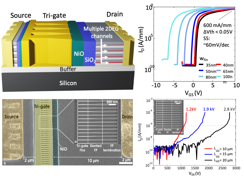
A. Esteghamat, …, E. Matioli, “2.7 kV E-Mode Multichannel GaN-on-Si based on p-type NiO/SiO2 Junction Tri-gate,” IEEE Electron Device Letters, 2025.

2022

T. Wang, Y. Zong, L. Nela and E. Matioli, “Enhancement-Mode Multi-Channel AlGaN/GaN Transistors With LiNiO Junction Tri-Gate,” IEEE Electron Device Letters, vol. 43, no. 9, pp. 1523–1526, 2022.

2022

L. Nela, A. Erine, A. M. Zadeh and E. Matioli, “Intrinsic Polarization Superjunctions: Design of Single and Multichannel GaN Structures,” IEEE Transactions on Electron Devices, vol. 69, no. 4, 2022.

2021

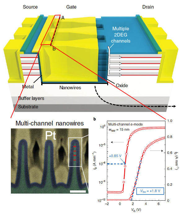
L. Nela, J. Ma, C. Erine, P. Xiang, T.-H. Shen, V. Tileli, T. Wang, K. Cheng and E. Matioli, “Multi-channel nanowire devices for efficient power conversion,” Nature Electronics, 2021.

2021

L. Nela, H. K. Yildirim, C. Erine, R. Van Erp, P. Xiang, K. Cheng and E. Matioli, “Conformal Passivation of Multi-Channel GaN Power Transistors for Reduced Current Collapse,” IEEE Electron Device Letters, 2021.

2021

P. Sohi et al., “Multi-channel AlGaN/GaN heterostructures,” Semiconductor Science and Technology, 2021.

2020

C. Erine, J. Ma, G. Santoruvo and E. Matioli, “Multi-channel AlGaN/GaN in-plane-gate field-effect transistors,” IEEE Electron Device Letters, vol. 41, no. 3, 2020.

2019

J. Ma, C. Erine, M. Zhu, L. Nela, P. Xiang, K. Cheng, E. Matioli, “1200 V Multi-Channel Power Devices with 2.8 Ω·mm ON-Resistance,” 2019 IEEE International Electron Devices Meeting (IEDM), San Francisco, CA, 2019.

2018

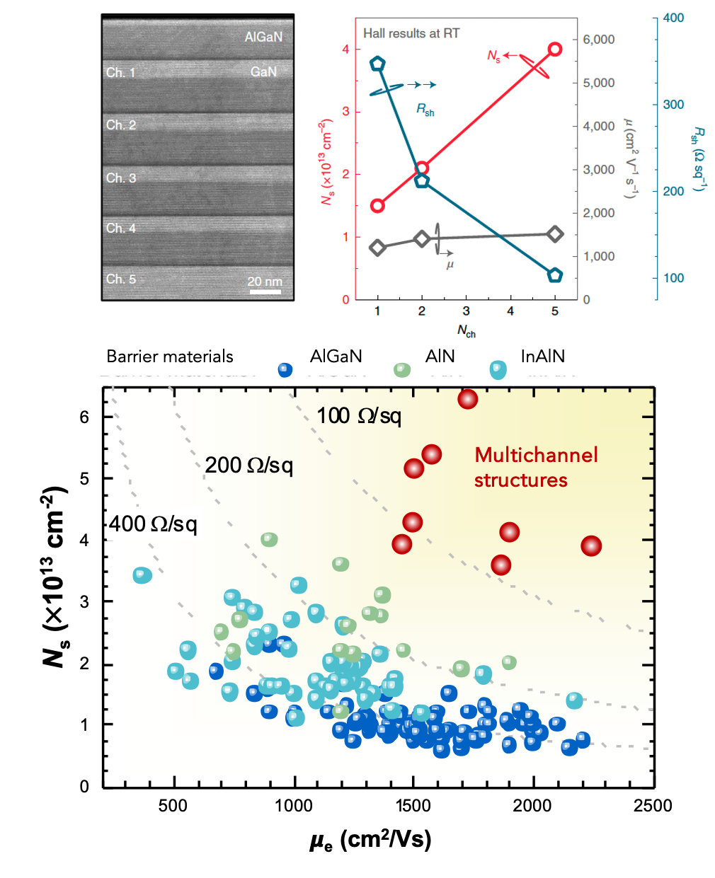
J. Ma, C. Erine, P. Xiang, K. Cheng and E. Matioli, “Multi-channel heterostructures,” Applied Physics Letters, vol. 113, no. 24, 242102, 2018.

2017

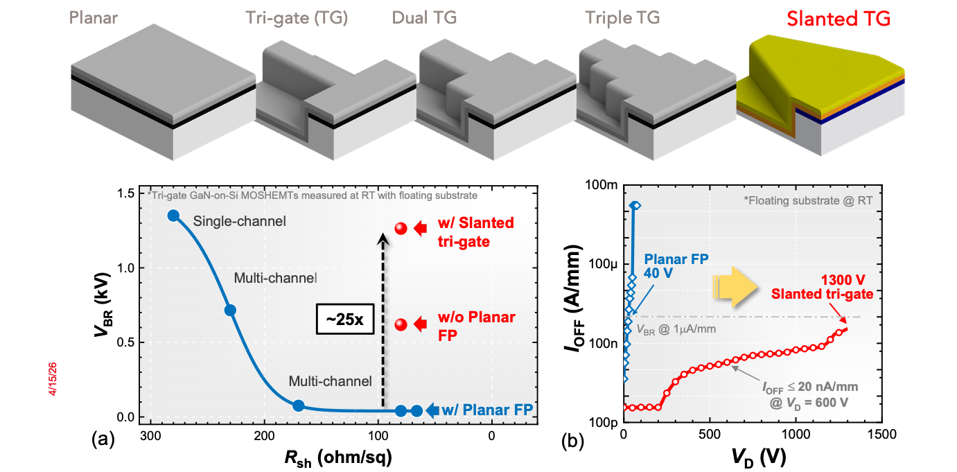
J. Ma and E. Matioli, “Slanted Tri-gates for High-Voltage GaN Power Devices,” IEEE Electron Device Letters, vol. 38, no. 9, 2017.

← Back to all research areas